![]()
Sometime ago, in this article (sorry still not in English), i described how nowadays the use of class G (or class H modulated) amplifiers for Hi-Fi installations could be a valid solution, also considering performances not only efficiency in terms of less current drawn from the mains and less dissipated power and finally heat. Modern components and some technical tricks allow to have a very smooth transition between rails, so that it is almost invisible at the scope as well; I would like to remember that, based on the IEC specifications for musical signals, above 5Khz we have only 4,5% of the total power

It will be very difficult for a class G amplifier working on the whole audio band the use of the higher supply voltage, so the possible problem of visible “glitches” on the waveforms does not arise.
Given this, looking at Douglas Self publications and browsing among some PRO amplifier schemas, I designed a small class G amplifier, which I thought to use in my HT setup, undecided between 5 mono units and a 5 channel one, even if I was not able to build them yet.
Here is the schema, like i put in LTSpice for simulation

It is a classic “mirror” topology with double differential input and double voltage amplifier stage (VAS), in an Emitter Follower configuration; also the output stage is an Emiter-Follower. So basically we have a classical and very well tested schema, capable to give very good distortion figures. The two supply voltages are 22/44 but we can use up to 25/50 without shatter the 2Ohm behavior.
The input stage uses the 2N5401/2N5550 pair, the same for the first VAS transistor, but we can use also the MPSA06/MPSA56, or others with the same pin layout. I used the BC547B/BC557B in the current mirrors, just keep in mind that changing the transistor here will change the associated VBE and finally the current that will flow at idle in the VAS: in that case some resistors will need to be changed to revert to the current schema values.
The input stage is biased at around 2.4mA per side and the VAS at around 7mA; each output stage transistor is biased at 30mA (but obviously You can change it); due to the high working current of the input stage it is highly degenerated with the 4 resistors marked {Rdeg}, which I set to 220Ohm. The remaining of the compensation is given by the to 68pF capacitors around the VAS.
Let’s take now a look at the output stage: the part working with the lower supply is a standard Emitter Follower with the MJE15034/MJE15035 as driver and the recent NJW1302/NJW3281 pair, basically another version of the famous MJL1302A/MJL3281A, but in a TO218 (TO3P) package instead of the TO264; it is possible to use whichever model in that case. On the PCB I’m working on I’m using a TO218 case, but we can use also the TO247 one which has almost about the same dimensions: the MJW1302/MJW3281 use that case (I have several of them).
The part of the output working with the higher supply is built with the same approach (E-F), but is configured to receive the required voltage swing to be activated. Unlike the old article, where the outer stage point of activation is given by a Zener in the bias chain (between the VAS and the VBE multiplier), in this schema I’m using the “bootstrapping” technique.
Basically the output voltage is connected to the higher supply rail by means of a zener biased by a resistor connected to that rail; the signal between the zener and the resistor is sent, through a diode, to the driver of the outer section, allowing it to start conduct before the output meet the lower supply. At this point the diode in series with the lower supply shut off and only the higher supply rail is modulated to the load. this stage is marked on the schema with “POS STEP” (“NEG STEP” for the negative side) together with a filter built on a 8.2KOhm resistor and two 150pF capacitors, which allow for an additional smooth transition with the rails at higher frequency: this filter is reported also on Patent #5387876.
The bootstrapping approach, instead of the one with the zener in the bias chain, allows to have a higher output voltage (and thus more power) because no additional V are lost before the output stage.
This is the 20Khz sin wave simulated with a 4Ohm load near the maximum power
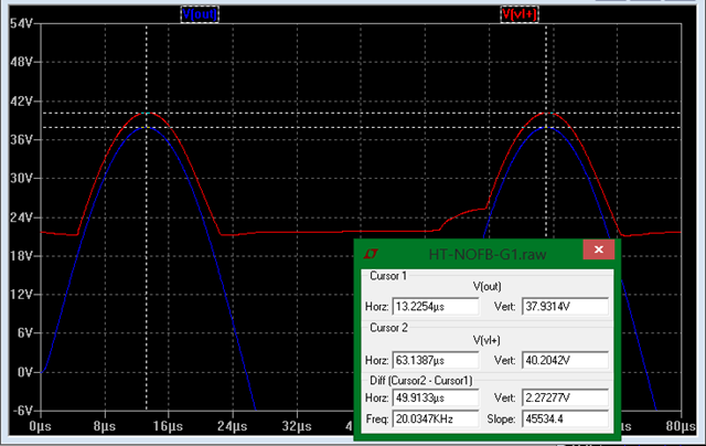
As You can see no “glitches” are present; on the second wave You can note a sort of bulge on the red data, which is a little anticipated voltage switch with smoother transition; on the first wave it is not visible but I’m pretty sure this is a limit of the simulation software. Going down with the frequency this bulge become less visible till vanish at around 10KHz, where the switch of the diode is not able to produce artifacts on the output signal; furthermore the better is the Shottky diode used the better is the switching behavior.
On the box over the waves You can see how the switched (sorry modulated 🙂 ) supply voltage is around 2.3V over the output signal; we could try to further “mask” the switch off behavior of the diode by increasing this difference. In the schema I used the 5,6V 3W 1N5919B zener, so due to its power rating we could increase its bias, or replace with for example the BZX84C6V2L and reducing the current in order to not go over its specification; using a 10KOhm resistor with the BZX the supply voltage settle to around 4V over the output. Do not set this difference too high because You will lower the overall efficiency. i the PRO world for example, where the rails are at least 45/90, tipical values are from 9V to 12V.
In the following two images we can see the comparison, in term of dissipated power and efficiency, between this class G amplifier and the same configured as a class B one, using only the higher supply voltage and continuing to use the whole 8 output power transistor. I set the total bias of the two schemas to be the same, so giving 60mA each output to the class G and 30mA each to the class B. the graphs were simulated using a 1Khz sin wave over an 8Ohm load.
Disspated power

Efficiency
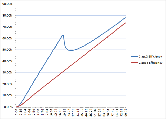
A remarkable difference, particularly at levels of average usage.
Let’s now see the differences with a real musical program: here LTSpice helps with its capability to load wave files as input signal; for this test I used 16s of the refrain of Lady Gaga “Poker Face” (where she starts with “Can’t read my, Can’t read my…”)
Class G
pout: AVG((v(out))*i(rout))=21.3676 FROM 0 TO 16
pdiss: AVG(((v(vpos)-v(vtrout))*ic(q24)*4)+((v(vl+)-v(vtrin))*ic(q19)*4))=18.5003 FROM 0 TO 16
Class B
pout: AVG((v(out))*i(rout))=21.3662 FROM 0 TO 16
pdiss: AVG((v(vpos)-v(vtrin))*ic(q24)*8)=36.2656 FROM 0 TO 16
We can see how the dissipated power of the class G is almost half that of class B; the difference is even higher for programs with higher dynamic excursion (like i verified with “Time” contained in the GOLD CD version of “Dark Side Of The Moon”).
A stereo module built on this circuit can be put inside a case like this http://www.modushop.biz/ecommerce/cat066.php?n=1 using an heatsink 30cm long, 4cm high and with fins of 3cm.
The main issue here is the power transformer, which should be difficult to find in order to be fitted in a 40mm case, due also to the fact the a good level of VA is required to correctly drive loads below 8Ohm.
I asked Canterbury Windings a couple of 160VA transformers with GOSS band and electrostatic screen between the primary ad the secondaries, with a total height of 38mm. This transformer has also been inserted in the available products and its model is
Type: TM155A
| Continuous power rating: 160VA |
| Primary: 230V @ 50Hz |
| Electrostatic screen |
| Secondaries: 4 x 16.5V @ 2.42A rms |
| GOSS band |
| Dimensions: approx 136x38mm |
| Mounting: M8 x 30mm bush in a potted centre |
| Extended lead time on this item |
At that time Terry told me that without the electrostatic screen some further VAs could be gained for the same dimension.
In the meanwhile I’m working to a PCB for a stereo module, with power supply included, separate bridge rectifiers and supply capacitor for each channel.
