Posts contrassegnato dai tag ‘amplifier’

Italiano

And some tests…

Recently I bought a couple of second hand Yamaha P7000S in order to driver a total of 4 bass units, built on the RCF L15P200AK-II woofer; like i did for other amplifiers in the past I took a look on on the Italian Mercatino Musicale site and found them in very good condition and for a reasonable price, little more than 700€ both. I was looking for a couple of amplifiers over a single unit of more power in order to have better flexibility in the configuration; I can use them all in stereo @8Ohm or bridged @4Ohm on two bass unit each. Moreover, considering that I currently use a CC4000 to drive the 12” mid basses in both 8 and 4 Ohm setup I can also try different configurations and for example use the CC4000 to drive the 4 bass units in 4Ohm stereo and the Yamahas for the 12”.

Also for this model, like my CC4000, I read several different comments both positive and negative on some forums; as usual in the choice I used my head and decided to give it a chance. Looking and the schematics on the net once again I found and amplifier with:

  • a good number of output devices, you can see a total of 12 per channel; better damping factor, less power per device, and so on …
  • a full transistor schema from the input to the output of the power module, while as usual input, filters and other “accessory” units are IC based. On most amplifiers the input stage of the power module is IC based; the P series is just like the Crest CA all transistor based, and with 1 capacitor through the whole signal path
  • an interesting power supply technology (EEEngine) which seems to be promising in terms of total power consumption and dissipated (= wasted); this translates into less heat generated.

Here is a shot of the internals

P7000S Internal

I haven’t had yet the chance to do a listening test and compare it to both the CA6 and the CC4000,but found some time to put it under a small bench; as usual I used my 8 2Ohm 50W resistors to build up a stereo 8Ohm load of 200W, which is capable of handling up to 1000W with a duty cycle of 5 (1s on 5 off). I then connected a small power distributor to the wall plug with 5m of 3×2.5mm2 cable and powered the unit, which has a 2m supply cable, quite small in my opinion; it’s a 3×0.75mm2 unit and maybe could “eat” some watts (read my CC4000 review for details). Maybe I’ll come back later on this.

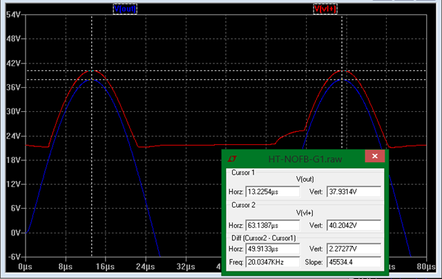
With the usual 3s on and 15s off @100Hz the P7000S clipped @675W/8Ohm, with the meter reading 73.5V RMS, the clip leds starting to light up and the wave figure like below

100Hz full power

The amplifier well met it’s specifications, which state 650W RMS for the EU version; yes the EU version (230V) seems to loose almost 50W compared to the other, and looking at the schematic this is due to a couple of inductors put in series on the main supply, which role sincerely is not so clear to me, even if on a forum i read that it should act like a PFC circuit, but PFC is something that is a little more complicated than a simple pair of inductors.

Supported by a video I saw on the net of a modded P7000S, and by a check on the schematic which confirmed me that their removal would produce only gains, I decided to disconnect the terminals of the coils and to put in place a jumper built with some cm of cable and a couple of faston; the non EU version have a jumper built on the board but it is the same.

I tested it again and got back around 740W 8Ohm, with the meter reading 77V RMS and the clip leds flashing lightly

100Hz full power no coils

As You can see the wave is still clean and this is very good; it seems that the removal of the coils not only give more power (65W) but also seems to present a better supply line to the switching modules and finally to the amps.

I then repeated the test @50Hz and the results were the same, if not slightly better (few mV more).

50Hz full power no coils

I currently do not have enough resistors to build  a proper 4Ohm load, so I cannot test such a high power unit without the risk of destroying the resistors, but I can test a 4Ohm bridge configuration with some safety margin; for this amplifier the sheet only report the bridge power for 4Ohm loads (2Ohm stereo) for 20ms peaks, and my objective was to have a unit which, when  bridged @4Ohm, just meet the RMS specs of my CA6 (currently 1650W) with some margin; so when used together they will deliver around 3200/3300W, and most important without pushing hard the amps to the limits; currently with the CA6 driving 2 bass units and with 2 satellites there is a very good sound balance, so with the whole 4+4 configuration the same balance will guaranteed, and also with a reasonable little margin to play a little harder when needed.

Given this I tried some tests with the bridged configuration @4Ohm and finally decided to stop at around 2350W RMS, that is 97V RMS; the two coils are still disconnected.

4Ohm bridged

This is more than enough form me, and the good thing is  that no breaker or other form of protection/limiting was kicking in; just remember that the CC4000 was triggering it’s circuit braker at around 2100W when bridged @4Ohm, so that I had to reduce the cycle to 1s on in order to be able to reach higher power levels.

As usual I also do some tests at higher frequencies to check for the absence of wave artifacts due to missconfigured idle current (higher distortion) or power supply residual; this time I was also curious about the behavior of the EEEngine.

This is the 10KHz wave at 2.83V RMS

2.83V @10K

And this is the same 10KHz wave at 80VPP (28.2RMS, 100W/8Ohm).

They are both clean; I then repeated the tests at 15Khz and the figures didn’t change, very clean the same.

I will order in the next days an additional resistors set in order to build a reliable 4Ohm load and will come back with the results under that load; moreover i think I will play around with the power chord.

Update on 08/12/2015

Today I replaced the power chord with a piece pf 3×2.5mmq cable, like You can see in this photo compared to the original.

20151125_090105

The results were almost the same, with the amplifier delivering 77.7V RMS @8Ohm (755W/8Ohm) at the onset of the clipping, confirming that the P7000S ,and also the P5000S I think, has a minimal sort of “regulation” for small undervoltage; the voltage at the board connectors was around 227V while with the original power chord it was around 222/223V.

20151208_151946

Here are some additional readings of this amplifier taken from the power box I use, just to get an idea of its power consumption

This is the at idle with no other equipment connected to the power box: 60VA

20151208_150243

This is at100W RMS @8Ohm both channels, with a total of additional 200VA used by a lamp, scope, pc and mixer; so around 470VA absorbed

20151208_151430

This is at 200W RMS @8Ohm both channels; around 800VA used

20151208_151615

And this is at full power @8Omh both channels: a total of around 1900VA for 1500W on the load

20151208_151931

Italiano 

Sometime ago, in this article (sorry still not in English), i described how nowadays the use of class G (or class H modulated) amplifiers for Hi-Fi installations could be a valid solution, also considering performances not only efficiency in terms of less current drawn from the mains and less dissipated power and finally heat. Modern components and some technical tricks allow to have a very smooth transition between rails, so that it is almost invisible at the scope as well; I would like to remember that, based on the IEC specifications for musical signals, above 5Khz we have only 4,5% of the total power

distribuzione potenza

It will be very difficult for a class G amplifier working on the whole audio band the use of the higher supply voltage, so the possible problem of visible “glitches” on the waveforms does not arise.

Given this, looking at Douglas Self publications and browsing among some PRO amplifier schemas, I designed a small class G amplifier, which I thought to use in my HT setup, undecided between 5 mono units and a 5 channel one, even if I was not able to build them yet.

Here is the schema, like i put in LTSpice for simulation

It is a classic “mirror” topology with double differential input and double voltage amplifier stage (VAS), in an Emitter Follower configuration; also the output stage is an Emiter-Follower. So basically we have a classical and very well tested schema, capable to give very good distortion figures. The two supply voltages are 22/44 but we can use up to 25/50 without shatter the 2Ohm behavior.

The input stage uses the 2N5401/2N5550 pair, the same for the first VAS transistor, but we can use also the MPSA06/MPSA56, or others with the same pin layout. I used the BC547B/BC557B in the current mirrors, just keep in mind that changing the transistor here will change the associated VBE and finally the current that will flow at idle in the VAS: in that case some resistors will need to be changed to revert to the current schema values.

The input stage is biased at around 2.4mA per side and the VAS at around 7mA; each output stage transistor is biased at 30mA (but obviously You can change it); due to the high working current of the input stage it is highly degenerated with the 4 resistors marked {Rdeg}, which I set to 220Ohm. The remaining of the compensation is given by the to 68pF capacitors around the VAS.

Let’s take now a look at the output stage: the part working with the lower supply is a standard Emitter Follower with the MJE15034/MJE15035 as driver and the recent NJW1302/NJW3281 pair, basically another version of the famous MJL1302A/MJL3281A, but in a TO218 (TO3P) package instead of the TO264; it is possible to use whichever model in that case. On the PCB I’m working on I’m using a TO218 case, but we can use also the TO247 one which has almost about the same dimensions: the MJW1302/MJW3281 use that case (I have several of them).

The part of the output working with the higher supply is built with the same approach (E-F), but is configured to receive the required voltage swing to be activated. Unlike the old article, where the outer stage point of activation is given by a Zener in the bias chain (between the VAS and the VBE multiplier), in this schema I’m using the “bootstrapping” technique.

Basically the output voltage is connected to the higher supply rail by means of a zener biased by a resistor connected to that rail; the signal between the zener and the resistor is sent, through a diode, to the driver of the outer section, allowing it to start conduct before the output meet the lower supply. At this point the diode in series with the lower supply shut off and only the higher supply rail is modulated to the load. this stage is marked on the schema with “POS STEP” (“NEG STEP”  for the negative side) together with a filter built on a 8.2KOhm resistor and two 150pF capacitors, which allow for an additional smooth transition with the rails at higher frequency: this filter is reported also on Patent #5387876.

The bootstrapping approach, instead of the one with the zener in the bias chain, allows to have a higher output voltage (and thus more power) because no additional V are lost before the output stage.

This is the 20Khz sin wave simulated with a 4Ohm load near the maximum power

As You can see no “glitches” are present; on the second wave You can note a sort of bulge on the red data, which is a little anticipated voltage switch with smoother transition; on the first wave it is not visible but I’m pretty sure this is a limit of the simulation software. Going down with the frequency this bulge become less visible till vanish at around  10KHz, where the switch of the diode is not able to produce artifacts on the output signal; furthermore the better is the Shottky diode  used the better is the switching behavior.

On the box over the waves You can see how the switched (sorry modulated 🙂 ) supply voltage is around 2.3V over the output signal; we could try to further “mask” the switch off behavior of the diode by increasing this difference. In the schema I used the 5,6V 3W 1N5919B zener, so due to its power rating we could increase its bias, or replace with for example the BZX84C6V2L and reducing the current in order to not go over its specification; using a 10KOhm resistor with the BZX the supply voltage settle to around 4V over the output. Do not set this difference too high because You will lower the overall efficiency. i the PRO world for example, where the rails are at least 45/90, tipical values are from 9V to 12V.

In the following two images we can see the comparison, in term of dissipated power and efficiency, between this class G amplifier and the same configured as a class B one, using only the higher supply voltage and continuing to use the whole 8 output power transistor. I set the total bias of the two schemas to be the same, so giving 60mA each output to the class G and 30mA each to the class B. the graphs were simulated using a 1Khz sin wave over an 8Ohm load.

Disspated power

Efficiency

A remarkable difference, particularly at levels of average usage.

Let’s now see the differences with a real musical program: here LTSpice helps with its capability to load wave files as input signal; for this test I used 16s of the refrain of Lady Gaga “Poker Face” (where she starts with “Can’t read my, Can’t read my…”)

Class G

pout: AVG((v(out))*i(rout))=21.3676 FROM 0 TO 16
pdiss: AVG(((v(vpos)-v(vtrout))*ic(q24)*4)+((v(vl+)-v(vtrin))*ic(q19)*4))=18.5003 FROM 0 TO 16

Class B

pout: AVG((v(out))*i(rout))=21.3662 FROM 0 TO 16
pdiss: AVG((v(vpos)-v(vtrin))*ic(q24)*8)=36.2656 FROM 0 TO 16

We can see how the dissipated power of the class G is almost half that of class B; the difference is even higher for programs with higher dynamic excursion (like i verified with “Time” contained in the GOLD CD version of “Dark Side Of The Moon”).

A stereo module built on this circuit can be put inside a case like this http://www.modushop.biz/ecommerce/cat066.php?n=1 using an heatsink 30cm long, 4cm high and with fins of 3cm.

The main issue here is the power transformer, which should be difficult to find in order to be fitted in a 40mm case, due also to the fact the a good level of VA is required to correctly drive loads below 8Ohm.

I asked Canterbury Windings a couple of 160VA transformers with GOSS band and electrostatic screen between the primary ad the secondaries, with a total height of 38mm. This transformer has also been inserted in the available products and its model is

Type: TM155A

Continuous power rating: 160VA
Primary: 230V @ 50Hz
Electrostatic screen
Secondaries: 4 x 16.5V @ 2.42A rms
GOSS band
Dimensions: approx 136x38mm
Mounting: M8 x 30mm bush in a potted centre
Extended lead time on this item


At that time Terry told me that without the electrostatic screen some further VAs could be gained for the same dimension.

In the meanwhile I’m working to a PCB for a stereo module, with power supply included, separate bridge rectifiers and supply capacitor for each channel.

Un po’ di tempo fa, in questo articolo, ho descritto come ormai l’impiego dei finali in classe G (o H modulata) in campo Hi-Fi possa considerarsi una soluzione adeguata anche considerando le performance, oltre che dal punto di vista dell’efficienza, sia come risparmio di corrente assorbita che come risparmio nella potenza dissipata e quindi calore generato. I moderni componenti disponibili e alcuni accorgimenti tecnici rendono lo switch tra una tensione e l’altra praticamente inavvertibile sulla forma d’onda anche alle frequenze più elevate; mi preme ricordare che in base alle specifiche IEC, per quanto riguarda un programma musicale, oltre i 5Khz rimane circa il 4,5% della potenza

distribuzione potenza

quindi risulterà molto difficile per un amplificatore in classe G che opera su tutta la banda utilizzare la tensione di alimentazione più alta, quindi l’eventuale problema di “glitches” presenti sulla forma d’onda non si pone.

Detto questo sfruttando le publicazioni di Douglas Self e curiosando tra alcuni schemi di finali professionale reperibili in rete, ho disegnato un piccolo finale in classe G, che avevo inizialmente previsto di utilizzare nel mio impianto HT, indeciso tra 5 componenti mono oppure un modulo a 5 canali, ma che non sono ancora riuscito a realizzare.

Di seguito lo schema, così come è stato inserito in LTSpice per la simulazione

image

Si tratta di una classica configurazione “mirror” con doppio differenziale d’ingresso e doppio amplificatore in tensione (VAS) in configurazione emitter follower; anche lo stadio d’uscita è un tipico emitter-follower. Quindi di base abbiamo di fronte uno schema abbastanza standard e collaudato, ma che è in grado di fornire ottime performance dal punto di vista della distorsione. Le due tensioni di alimentazione sono 22/44 ma ci si può tranquillamente spingere fino a 25/50 senza pregiudicare il funzionamento su 2Ohm, se  per caso si pensa di usare questo carico.

il differenziale di ingresso usa la coppia 2N5401/2N5550, cosi come il primo transistor del VAS, ma si possono usare indifferentemente anche gli MPS06/MPSA56 o altri dalla piedinatura identica; per lo specchio di corrente (current mirror) ho usato i BC547B/BC557B, tenete solo presente che cambiando transistor cambia la tensione VBE e quindi di conseguenza la corrente che scorrerà nel VAS, per cui sarà necessario modificare il valori di alcune resistenze. Ricordatevi che i transistor BC hanno la piedinatura invertita rispetto agli MPSA e 2N…

Per quanto riguarda la corrente di lavoro lo stadio di ingresso è polarizzato a circa 2.4mA per ramo mentre il VAS a circa 7mA per ramo; i finali invece operano con una corrente di riposo di circa 30mA (nulla vieta di cambiarla). Data l’elevata corrente di lavoro dello stadio di ingresso lo stesso è fortemente degenerato dalle 4 resistenze chiamate {Rdeg} il cui valore è 220Ohm, al fine di mantenere la stabilità di funzionamento; il resto della compensazione è fornito dal doppio condensatore da 68pF presente nel VAS.

Vediamo ora il funzionamento dello stadio finale: la parte che lavora alla tensione più bassa è un normale emitter follower, con gli MJE15034/MJE15035 come driver e i recenti NJW1302/NJW3281, praticamente una versione riveduta degli MJL1302/MJL3281 nel contenitore TO218 invece che nel TO264, ma praticamente è possibile usare qualsiasi modello disponibile in tale contenitore. Nel PCB che sto preparando ho previsto finali in contenitore TO218 (come gli NJW e simili) oppure TO247 che ha praticamente la stessa dimensione; tra i transistor in TO247 ci sono gli MJW1302/MJW3281.

La parte che lavora alla tensione superiore è fatta allo stesso modo, ma configurata per ricevere il necessario swing di tensione al fine di attivarsi; a differenza del precedente articolo, dove in sostanza la polarizzazione dello stadio a tensione più elevata avviene tramite degli Zener nella catena di bias del finale (tra i due transitor del VAS), nello schema descritto qui ho adottato la cosiddetta tecnica di “bootstrapping”.

In sostanza l’uscita dell’ampli è collegata alla tensione più alta tramite uno zener polarizzato da una resistenza; il segnale presente tra la resistenza e lo zener vine inviato, tramite un diodo, al driver dello stadio ad tensione più elevata, facendolo entrare in conduzione qualche V prima che l’uscita raggiunga la tensione di alimentazione più bassa. A questo punto il diodo in serie alla tensione più bassa viene “spento” e sul carico fluisce solo la tensione più alta. Questo stadio è racchiuso nel riquadro “POS STEP” (“NEG STEP” per il ramo negativo), unitamente ad un filtro composto dalla resistenza da 8.2K e dai due condensatori da 150pF, che rendono ancora più morbido lo switch tra le due tensioni alle frequenze più alte; in realtà questo filtro è citato anche nel Patent N. 5387876.

Il meccanismo di bootstrapping rispetto a quello visto nell’altro articolo permette di avere a disposizione una maggiore tensione in uscita (e quindi maggiore potenza) in quanto non si perdono i Volts di caduta sugli zener nel VAS + circuito di polarizzazione dei finali.

Questa è la sinusoide simulata a 20Khz su un carico di 4Ohm in prossimità della massima potenza d’uscita

image

Come si può vedere la sinusoide non presenta “glithces”; sulla seconda semionda è presente un leggero rigonfiamento che causa una sorta di anticipo nel cambio di tensione, rendendolo ancora più morbido. Sulla prima semionda tale rigonfiamento non è presente, ma sono sicuro che si tratta di un limite del software di simulazione. Scendendo con la frequenza il rigonfiamento si riduce progressivamente fino a sparire del tutto a quelle frequenze (<10Khz) dove lo switch del diodo presente sulla tensione più bassa non è più percepibile sulla forma d’onda anche senza l’uso del filtro citato sopra

Nel riquadro si nota come la tensione di alimentazione sia poco più di 2V al di sopra di quella di uscita. Volendo migliorare ulteriorimente il comportamento durante il cambio di tensione i potrebbe adottare uno zener di valore nominare più alto, perdendo un po’ in termini di efficienza; nel mio schema ho usato un 1N5919B da 5,6V 3W, per il quale aumentando la polarizzazione si può ottenere un’ulteriore innalzamento della tensione al di sopra di quella di uscita.

Nei due grafici seguenti vediamo il confronto in termini di efficienza e potenza dissipata del finale in oggetto confrontato con un finale in classe B, ottenuto praticamente dal primo togliendo l’alimentazione più bassa, connettendo gli otto transistor finali (4 per ramo) in modo classico, e regolando il bias totale per farlo coincidere con quello del finale in classe G, dove in assenza di segnale lavorano praticamente solo 4 transistor invece che 8. I grafici sono stati simulati con segnale sinusoidale ad 1KHz su carico di 8Ohm.

Potenza dissipata

image

Efficienza

image

Una notevole differenza, soprattutto nella zona che corrisponde all’utilizzo medio.

Vediamo ora le differenze con un programma musicale: qui ci viene in aiuto LTSpice che permette di specificare in input un file .WAV. Per questo test ho usato 16s di ritornello di Poker Face di Lady Gaga

Classe G

pout: AVG((v(out))*i(rout))=21.3676 FROM 0 TO 16
pdiss: AVG(((v(vpos)-v(vtrout))*ic(q24)*4)+((v(vl+)-v(vtrin))*ic(q19)*4))=18.5003 FROM 0 TO 16

Classe B

pout: AVG((v(out))*i(rout))=21.3662 FROM 0 TO 16
pdiss: AVG((v(vpos)-v(vtrin))*ic(q24)*8)=36.2656 FROM 0 TO 16

Abbiamo quindi una dissipazione ridotta a metà a parità di potenza erogata; se prendiamo poi un brano con una dinamica maggiore il divario è ancora più evidente.

Un modulo stereo che utilizza questo circuito può essere tranquillamente inserito in un contenitore di questo tipo http://www.modushop.biz/ecommerce/cat066.php?n=1 utilizzando un dissipatore lungo 300mm, alto 40mm (la massima altezza interna disponibile) e con le alette profonde 30mm.

Il problema principale rimane il trasformatore, che dovendo avere comunque una potenza adeguata per gestire al meglio i moduli più bassi, risulta di difficile costruzione; io mi ero fatto costruire da Canterbury Windings due trasformatori da 160VA l’uno con anello amagnetico esterno e schermo elettrostatico tra primario e secondari, per un’altezza totale di 38mm. il trasformatore è stato poi inserito tra i prodotti disponibili con questa sigla

Type: TM155A

Continuous power rating: 160VA
Primary: 230V @ 50Hz
Electrostatic screen
Secondaries: 4 x 16.5V @ 2.42A rms
GOSS band
Dimensions: approx 136x38mm
Mounting: M8 x 30mm bush in a potted centre
Extended lead time on this item


Terry all’epoca mi aveva detto che rinunciando allo schermo elettrostatico si possono ottenere un po’ di VA in più.

Nel frattempo sto completanto anche il PCB per un modulo stereo completo di alimentatore