In questo articolo vediamo come usare il software di misura Smaart con il mixer Behringer XR18, senza ricorrere ad ulteriori schede audio; la stesso principio può essere applicato anche alla versione X18 e X32, cosi come ad esempio ai modelli Midas MR18 e M32, con i quali fondamentalmente condivide il principio di funzionamento (Midas e Behringer e molti altri fanno parte della holding Music Tribe, fondata da Uli Behringer) .
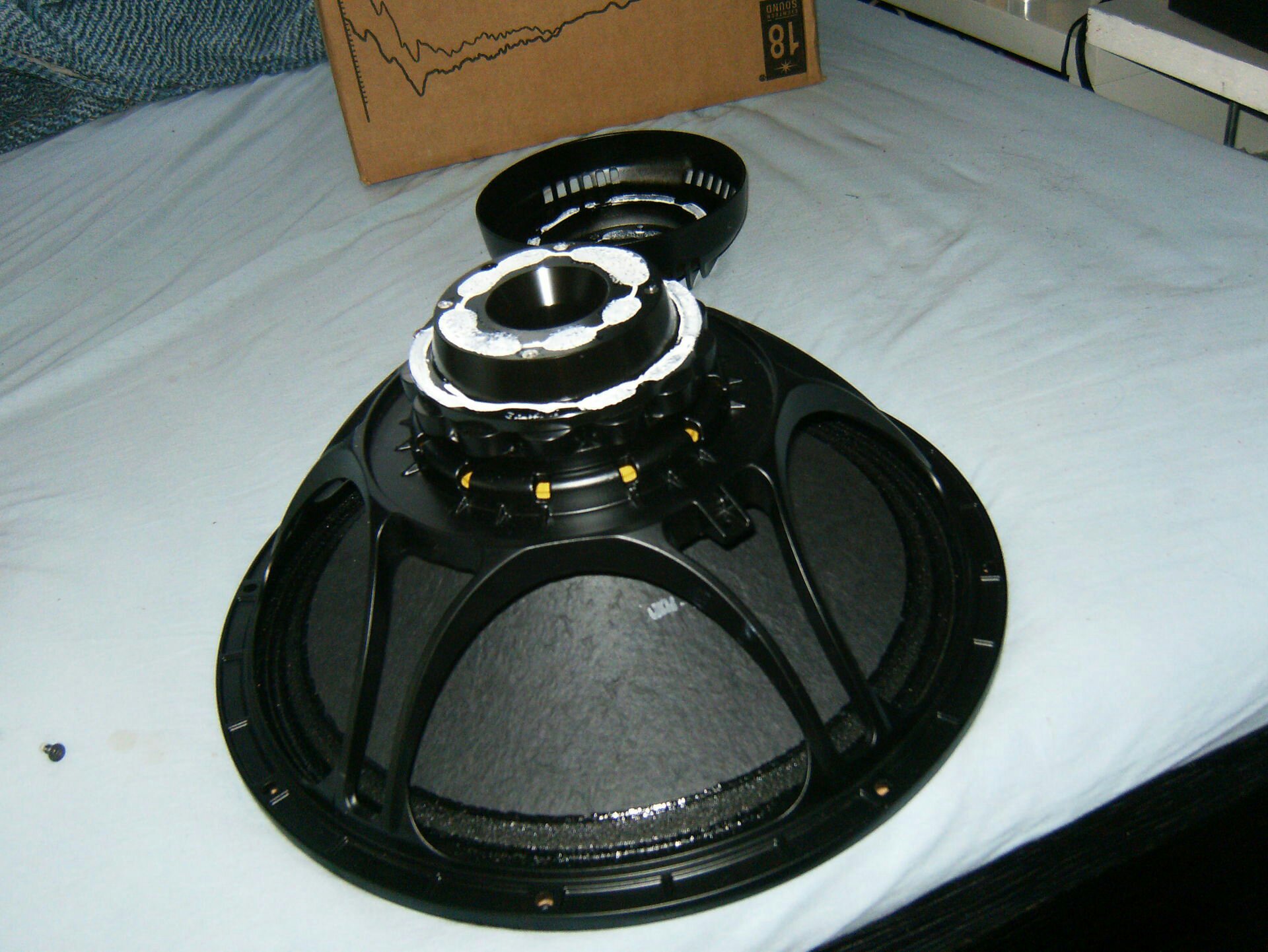
Grazie all’ingresso USB il Behringer XR18 può essere usato sia come un registratore a 16 tracce oppure come una scheda audio 8+8, 8 ingressi e 8 uscite; ed è proprio questa caratteristica che può essere sfruttata per configurare Smaart e misurare la “transfer function” di un diffusore (risposta + fase), oppure per allineare SUB e satelliti, SUB nelle varie configurazioni (End- Fire, Gradiente, Cardioide) e attività simili.
Smaart, attualmente alla versione V8, è un software di analisi FFT multicanale universalmente impiegato in campo audio professionale da diversi anni, dal costo di circa 1000$, che successivamente è stato affiancato da Smart DI in versione a soli 2 canali; nel caso in cui non sia necessario misurare la risposta in più punti, ad esempio fronte e retro di un subwoofer cardiode, offre le stesse funzionalità ad un costo decisamente inferione, 600$, differenza non da poco nel caso di impiego a livello hobbystico/dilettantistico. Sono comunque disponibili le versioni demo dei due software, ed in questo periodo di emergenza sanitaria la valutazione è stato estesa a 90 giorni rispetto ai canonici 30.
Mi fa estremamente piacere inoltre riportare che RCF nella sua recente versione 4.0 del software RDNet, per la gestione dei diffusori che lo supportano, ha introdotto la stessa funzionalità e per di più in modo del tutto gratuito, è sufficiente registrarsi sul sito per procedere al download e all’installazione del software; in un prossimo articolo vedremo anche come usare RDNet per ottenere gli stessi risultati.
Fatta questa introduzione veniamo alla parte pratica dell’articolo iniziando ad installare tutto quello che ci serve:
- Smaart V8 dal seguente link https://www.rationalacoustics.com/smaart/demo-smaart/download-smaart-demo/ previa registrazione
- X-Air Edit (PC) dal seguente link https://www.behringer.com/product.html?modelCode=P0BI8 cliccando su Software sotto Product Library sulla destra della pagina
- I driver ASIO specifici per il mixer prelevandoli dalla stessa posizione del punto precedente
Una volta completata l’installazione passiamo alla configurazione iniziando da Smaart, che tra l’altro essendo in versione demo non permette di salvare i settaggi e ad ogni apertura del programma si riparte da 0
All’apertura ci viene chiesto di configurare Input e Output: questo il dettaglio dell’ Input con selezionati i canali 1 e 2

Per comodità sull’ Ouput ho messo i canali 15 e 16, ma può essere usato qualsiasi altro canale; oltre all’ingresso AUX dell’ XR18 ho al massimo 10/12 canali usati, così in caso di necessità mi posso tenere salvata la configurazione.

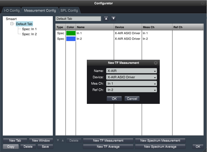
Fatto questo bisogna passare sulla pagina “Measurement Config” e creare una nuova configurazione cliccando sul pulsante “New TF Measurement”
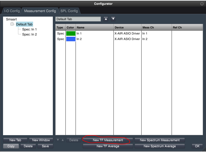
Diamo un nome e poi OK e di nuovo OK per chiudere il configuratore
Sulla schermata principale poi bisogna cliccare sul pulsante “Transfer” per arrivare alla schermata che ci serve per le misure
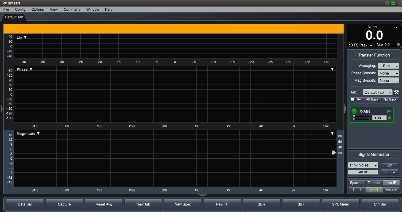
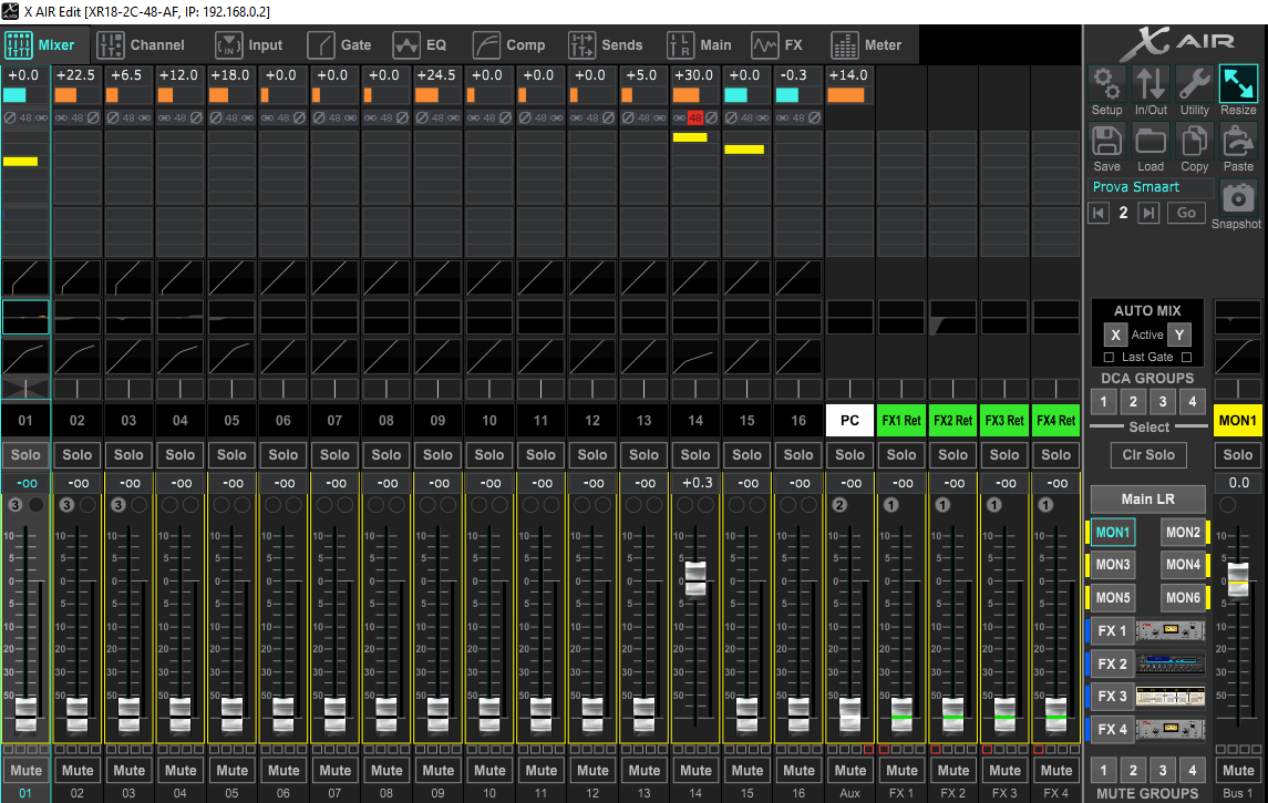
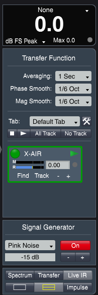
L’ultima configurazione necessaria su Smaart a questo punto è quella del generatore; cliccando su “Signal Generator” si apre la relativa finestra e qui io ho impostato il livello di segnale a -15dB e abilitato anche l’uscita “Aux” tramite il canale 16, cosi da ritrovarmi lo stesso segnale sulle uscite L e R del mixer.
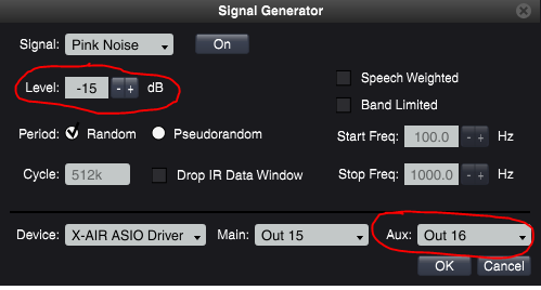
Passando al Behringer XR18 e al suo software partiamo dal canale 14 al quale ho deciso di collegare il microfono Behringer ECM8000, configurato con un guadagno di +30dB ed il Phantom Power +48V acceso; nell’immagine si vede anche il livello del canale 15 impostato a 0dB (Main out di Smaart) e il master a -8dB, ma quest’ultimo è arbitrario e dipende dal volume globale

Il canale 15, che ricordiamo essere il “Master” di Smaart, deve essere configurato per ricevere il segnale dall’ingresso USB e non da quello analogico, in questo modo

Adesso dobbiamo fare in modo di rimandare a Smaart i 2 segnali, quello del CH14 del microfono che rappresenta la “misura” e quello che arriva dal master sul CH15, che oltre ad andare ad alimentare le casse deve tornare come “riferimento”; per questo ci fanno comodo le uscite BUS dell’ XR18 che però in questo caso devono essere dirottate ai canali USB Send del mixer, come evidenziato nelle prossime 3 immagini.
Configurazione degli USB Send per mandare il BUS1 e il BUS2 agli ingressi 1 e 2 configurati in Smaart
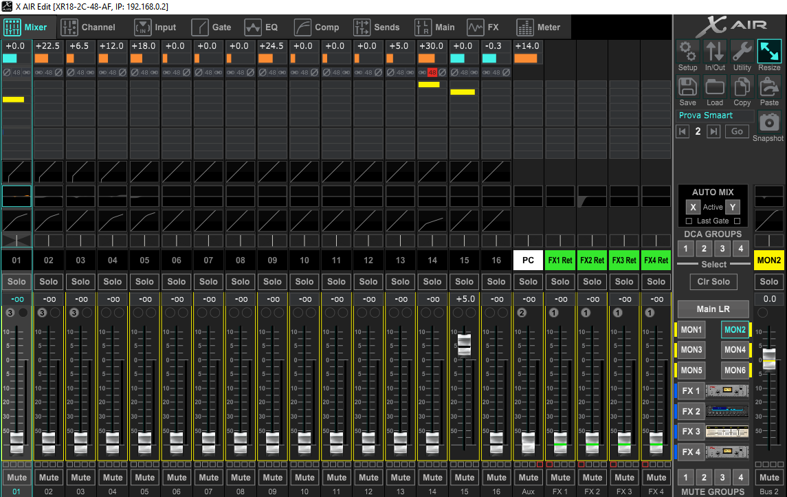
Dalla finestra principale di X-Air Edit cliccando in alto a destra su In/Out e poi su USB Send dobbiamo configurare BUS1 e BUS2 per andare su USB 1 e USB 2.

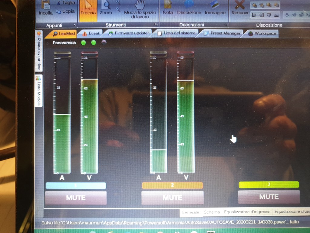
A questo punto è chiudiamo la finestra In/Out ed è tutto pronto per potere catturare le nostre misure, l’unica cosa che conviene fare prima di procedere è tarare il segnale di riferimento in Smaart, per evitare che sia troppo basso o troppo alto. Per fare questo bisogna accendere il generatore di segnale e verificare che il segnale di riferimento abbiamo un valore opportuno, come nell’immagine seguente, dove siamo appena al limite della zona gialla per il riferimento (R); in caso di necessità si può agire o sul livello del generatore oppure sui livelli del mixer. Successivamente si dovrà regolare il livello del segnale in arrivo dal microfono (M) per essere molto simile al riferimento e avere un grafico a cavallo dello 0dB
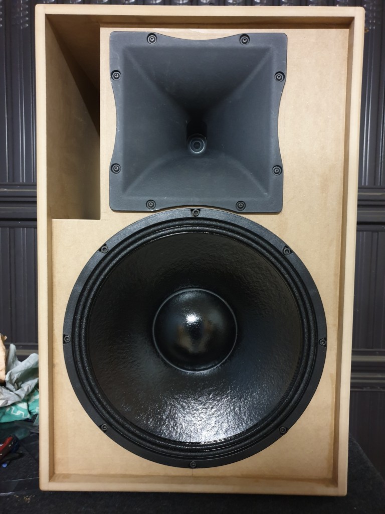
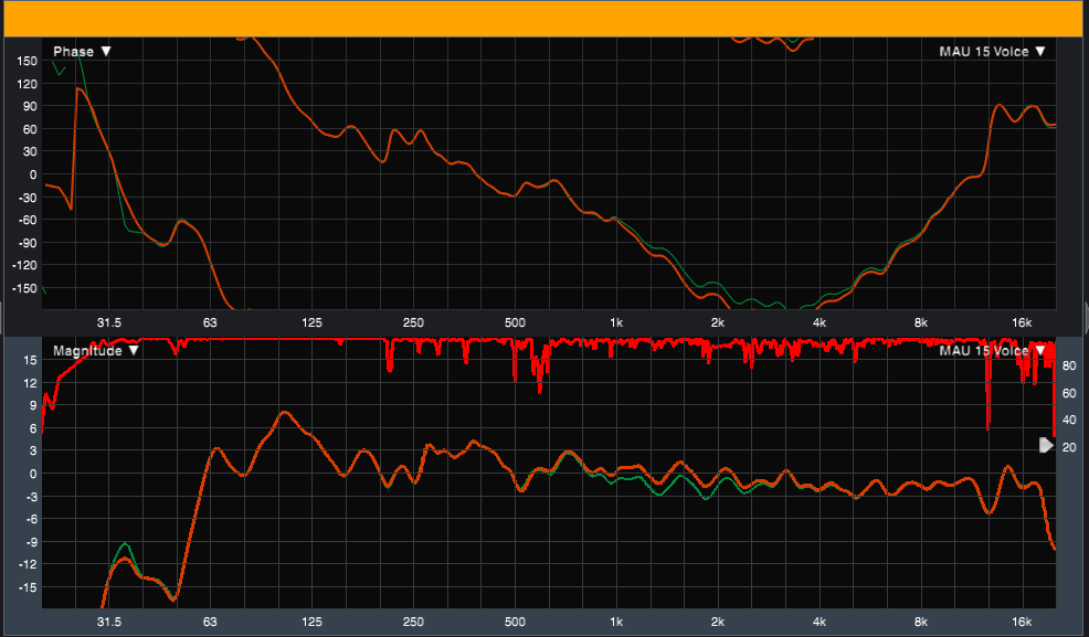
Di seguito un immagine di alcune misure fatte in ambiente su 3 diversi diffusori: RCF ART-715 MK4 (Giallo), Yamaha DSR 115 (Rosso) e la mia cassa con 18Sound 15ND930 + RCF ND840 su tromba HF94 e Powersoft Litemod (Verde).